Description
These are the reference designs for the FPGA Drive FMC Gen4 and M.2 M-key Stack FMC adapters that allow connecting NVMe SSDs and other M.2 M-key modules to FPGA, MPSoCs and APACs via the FPGA Mezzanine Card (FMC) connector.
Both of the FMC cards shown below can be used with these reference designs.
FPGA Drive FMC Gen4 |
M.2 M-key Stack FMC |
|---|---|
|
|


Hardware Platforms
The hardware designs provided in this reference are based on Vivado and support a range of FPGA, MPSoC and ACAP evaluation boards. The repository contains all necessary scripts and code to build these designs for the supported platforms listed below:
FPGA platforms
Target board |
FMC Slot |
Active |
PCIe IP |
Standalone |
PetaLinux |
|---|---|---|---|---|---|
HPC |
1x |
✅ |
❌ |
||
LPC |
1x |
✅ |
❌ |
||
HPC |
2x |
✅ |
❌ |
||
LPC |
1x |
✅ |
❌ |
||
HPC1 |
1x |
✅ |
❌ |
||
HPC2 |
1x |
✅ |
❌ |
||
HPC |
1x |
✅ |
❌ |
||
FMCP |
2x |
✅ |
❌ |
Zynq-7000 platforms
Target board |
FMC Slot |
Active |
PCIe IP |
Standalone |
PetaLinux |
|---|---|---|---|---|---|
LPC |
1x |
✅ |
✅ |
||
LPC |
1x |
✅ |
✅ |
||
HPC |
1x |
✅ |
✅ |
||
LPC |
1x |
✅ |
✅ |
Zynq UltraScale+ platforms
Target board |
FMC Slot |
Active |
PCIe IP |
Standalone |
PetaLinux |
|---|---|---|---|---|---|
HPC |
2x |
✅ |
✅ |
||
LPC |
1x |
✅ |
✅ |
||
HPC0 |
2x |
✅ |
✅ |
||
HPC1 |
1x |
✅ |
✅ |
||
FMCP |
2x |
✅ |
✅ |
||
FMCP |
2x |
✅ |
✅ |
||
FMCP |
2x |
✅ |
✅ |
Versal platforms
Target board |
FMC Slot |
Active |
PCIe IP |
Standalone |
PetaLinux |
|---|---|---|---|---|---|
FMCP1 |
2x |
✅ |
✅ |
||
FMCP2 |
2x |
✅ |
✅ |
||
FMCP |
1x |
✅ |
✅ |
||
FMCP1 |
2x |
✅ |
✅ |
||
FMCP2 |
2x |
✅ |
✅ |
||
FMCP |
2x |
✅ |
✅ |
||
FMCP |
1x |
✅ |
✅ |
||
FMCP |
1x |
✅ |
✅ |
PCIe IP
These designs implement one PCIe root complex per active M.2 slot. All designs make use of the integrated PCIe blocks that are built into the FPGA, MPSoC or ACAP device. The PCIe IP core used in each design depends on the device and is indicated in the “PCIe IP” column in the tables above.
The table below lists the PCIe IP cores used in these designs and provides links to their product pages. As all of these IP make use of hard PCIe blocks that are integrated into the FPGA/MPSoC/ACAP devices, they do not require a license to use.
IP Label |
IP Name |
|---|---|
axi_pcie |
|
axi_pcie3 |
|
xdma |
|
qdma |
Active M.2 Slots
Some of the designs have only one active M.2 slot due to limitations of the target board. The table below illustrates how to load the M.2 slots for designs that can support only one M.2 module vs those that can support two.
One Active Slot |
Two Active Slots |
|---|---|
|
|
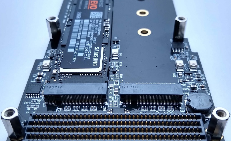
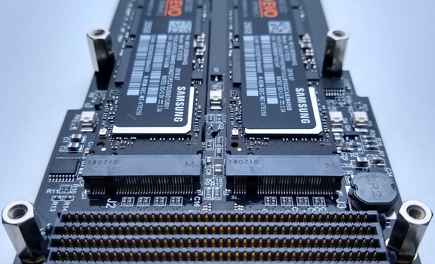
When using designs with only one active slot, you must leave the slot labelled “SLOT 2” or “SSD2” unloaded.
Software
These reference designs can be driven by either a standalone application or within a PetaLinux environment. The repository includes all necessary scripts and code to build both environments. The table below outlines the corresponding applications available in each environment:
Environment |
Available Applications |
|---|---|
Standalone |
PCIe enumeration test |
PetaLinux |
Built-in Linux commands |
The standalone software application reports on the status of the PCIe link and performs enumeration of the detected PCIe end-points (ie. the M.2 modules).