Stand-alone Application
A stand-alone software application can be built for this project using the build script contained in the Vitis subdirectory of this repo. The build script creates a Vitis workspace containing the hardware platform (exported from Vivado) and a stand-alone application. The application originates from an example provided by Xilinx which is located in the Vitis installation files. The program demonstrates basic usage of the stand-alone driver including how to check link-up, link speed, the number of lanes used, as well as how to perform PCIe enumeration. The original example applications can be viewed on the embeddedsw Github repo:
For the AXI PCIe designs: xaxipcie_rc_enumerate_example.c
For the XDMA and QDMA designs: xdmapcie_rc_enumerate_example.c
Note that the repo carries lightly modified copies of these examples in
Vitis/common/src/ (see advanced for the modifications).
Building the Vitis workspace
To build the Vitis workspace and example application, you must first generate the Vivado project hardware design (the bitstream) and export the hardware. Once the bitstream is generated and exported, then you can build the Vitis workspace using the provided scripts. Follow the build instructions — the steps are the same on Windows and Linux.
Hardware setup
Before running the application, you will need to setup the hardware.
Connect one or more SSDs to the mezzanine card and then plug it into the target board. Instructions for doing this can be found in the Getting started guide.
To receive the UART output of this standalone application, you will need to connect the USB-UART of the development board to your PC and run a console program such as Putty.
For Microblaze designs: The UART speed must be set to 9600.
For Zynq-7000, Zynq UltraScale+ and Versal designs: The UART speed must be set to 115200.
Run the application
You must have followed the build instructions before you can run the application.
Launch the Xilinx Vitis GUI.
When asked to select the workspace path, select the
Vitis/<target>_workspacedirectory.Power up your hardware platform and ensure that the JTAG is connected properly.
In the Vitis Explorer panel, double-click on the System project that you want to run - this will reveal the application contained in the project. The System project will have the postfix “_system”.
Now right click on the application “ssd_test” then navigate the drop down menu to Run As->Launch on Hardware (Single Application Debug (GDB))..
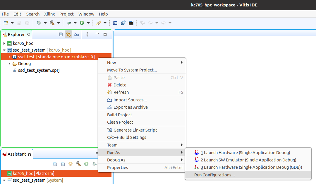
The run configuration will first program the FPGA with the bitstream, then load and run the application. You can view the UART output of the application in a console window and it should appear as follows:
Output of XDMA designs
Zynq MP First Stage Boot Loader
Release 2025.2   May 14 2026  -  14:56:34
PMU-FW is not running, certain applications may not be supported.
Interrupts currently enabled are        0
Interrupts currently pending are        0
Interrupts currently enabled are        0
Interrupts currently pending are        0
Link is up
Bus Number is 00
Device Number is 00
Function Number is 00
Port Number is 00
PCIe Local Config Space is   100147 at register CommandStatus
PCIe Local Config Space is    70100 at register Prim Sec. Bus
Root Complex IP Instance has been successfully initialized
xdma_pcie:
PCIeBus is 00
PCIeDev is 00
PCIeFunc is 00
xdma_pcie: Vendor ID is 10EE
Device ID is 9131
xdma_pcie: This is a Bridge
xdma_pcie: bus: 00, device: 00, function: 00: BAR 0 is not implemented
xdma_pcie: bus: 00, device: 00, function: 00: BAR 1 is not implemented
xdma_pcie:
PCIeBus is 01
PCIeDev is 00
PCIeFunc is 00
xdma_pcie: Vendor ID is 144D
Device ID is A80A
xdma_pcie: This is an End Point
xdma_pcie: bus: 01, device: 00, function: 00: BAR 0, ADDR: 0xA1000000 size : 16K
xdma_pcie: bus: 01, device: 00, function: 00: BAR 1required IO space; it is unassigned
xdma_pcie: bus: 01, device: 00, function: 00: BAR 2 is not implemented
xdma_pcie: bus: 01, device: 00, function: 00: BAR 3 is not implemented
xdma_pcie: bus: 01, device: 00, function: 00: BAR 4 is not implemented
xdma_pcie: bus: 01, device: 00, function: 00: BAR 5 is not implemented
xdma_pcie: End Point has been enabled
Successfully ran XdmaPcie rc enumerate Example
Output of AXI PCIe designs
Interrupts currently enabled are        0
Interrupts currently pending are        0
Interrupts currently enabled are        0
Interrupts currently pending are        0
Link is up
Bus Number is 00
Device Number is 00
Function Number is 00
Port Number is 00
PCIe Local Config Space is   100147 at register CommandStatus
PCIe Local Config Space is    70100 at register Prim Sec. Bus
Root Complex IP Instance has been successfully initialized
Start Enumeration of PCIe Fabric on This System
PCIeBus is 00
PCIeDev is 00
PCIeFunc is 00
Vendor ID is 10EE
This is a Bridge
PCIeBus is 01
PCIeDev is 00
PCIeFunc is 00
Vendor ID is 144D
This is an End Point
End Point has been enabled
End of Enumeration of PCIe Fabric on This system
Successfully ran Axipcie rc enumerate Example
Output of the QDMA designs
VADJ: 1.5V enabled successfully
Interrupts currently enabled are        0
Interrupts currently pending are        0
Interrupts currently enabled are        0
Interrupts currently pending are        0
Link is up
Bus Number is 00
Device Number is 00
Function Number is 00
Port Number is 00
PCIe Local Config Space is        0 at register CommandStatus
PCIe Local Config Space is        0 at register Prim Sec. Bus
Root Complex IP Instance has been successfully initialized
xdma_pcie:
PCIeBus is 00
PCIeDev is 00
PCIeFunc is 00
xdma_pcie: Vendor ID is 10EE
Device ID is B048
xdma_pcie: This is a Bridge
xdma_pcie: Requested BAR size of 4292870144K for bus: 00, dev: 00, function: 00 is out of range
                xdma_pcie:
PCIeBus is 01
PCIeDev is 00
PCIeFunc is 00
xdma_pcie: Vendor ID is 144D
Device ID is A80A
xdma_pcie: This is an End Point
xdma_pcie: bus: 01, device: 00, function: 00: BAR 0, ADDR: 0xA8000000 size : 16K
xdma_pcie: bus: 01, device: 00, function: 00: BAR 1required IO space; it is unassigned
xdma_pcie: bus: 01, device: 00, function: 00: BAR 2 is not implemented
xdma_pcie: bus: 01, device: 00, function: 00: BAR 3 is not implemented
xdma_pcie: bus: 01, device: 00, function: 00: BAR 4 is not implemented
xdma_pcie: bus: 01, device: 00, function: 00: BAR 5 is not implemented
xdma_pcie: End Point has been enabled
Successfully ran XdmaPcie rc enumerate Example
Changing Target Slot
In designs that support two M.2 slots, you can change the target slot by modifying a define value in the example application. The tables below show the lines to modify and their potential values.
AXI PCIe designs |
XDMA and QDMA designs |
|
|---|---|---|
File to modify |
|
|
Define |
XPAR_XAXIPCIE_0_BASEADDR |
XPAR_XXDMAPCIE_0_BASEADDR |
M.2 Slot 1 |
XPAR_XAXIPCIE_0_BASEADDR |
XPAR_XXDMAPCIE_0_BASEADDR |
M.2 Slot 2 |
XPAR_XAXIPCIE_1_BASEADDR |
XPAR_XXDMAPCIE_1_BASEADDR |
Advanced Design Details
Linker script modifications for MicroBlaze designs
For the MicroBlaze designs, the Vitis linker script generator may assign sections across multiple memory regions. To ensure the application runs correctly, the Vitis build script modifies the generated linker script and reassigns all sections to local memory.
If you want to manually create an application in the Vitis for one of the MicroBlaze designs, you will have to manually modify the automatically generated linker script, and set all sections to local memory.
axipcie driver
This project uses a modified version of the axipcie driver.
The axipcie_v3_4 driver is used by designs that use the AXI Memory Mapped to PCIe IP (axi_pcie) and
designs that use the AXI PCIe Gen3 IP (axi_pcie3). However, the driver’s SDT device tree binding file
axipcie_v3_4/data/axipcie.yaml only declares the compatible string xlnx,axi-pcie-host-1.00.a, which
matches the older AXI Memory Mapped to PCIe IP. It does not include xlnx,axi-pcie3-3.0, which is the
compatible string used by the AXI PCIe Gen3 IP in the device tree. As a result, the SDT driver mapping
fails to associate the IP with the axipcie driver, and the BSP is built without the driver.
Our modified version of axipcie.yaml adds xlnx,axi-pcie3-3.0 as a compatible string so that the
driver is correctly included in the BSP for designs that use the AXI PCIe Gen3 IP.
Additionally, the YAML references xlnx,port-type for the root complex detection field, but the device
tree uses xlnx,dev-port-type. Our patch corrects this so that the IncludeRootComplex field in the
config table is populated correctly. However, the device tree value for root port designs is 2 (PCI
Express Root Port), while the driver expects 1 (XAXIPCIE_IS_RC). The example application normalizes
any non-zero value to 1 after initialization to satisfy the driver’s internal assertions.
xdmapcie driver
This project uses a modified version of the xdmapcie driver.
The xdmapcie_v3_1 driver is used by designs that use the QDMA IP. The driver’s CfgInitialize function
contains hardcoded address values for swapping the ECAM (PCIe config space) and CSR (control/status register)
base addresses. These hardcoded values do not match the address map of this project’s designs, causing the
driver to access the wrong address regions. Specifically, local config space reads/writes and PCIe fabric
enumeration fail because the driver’s BaseAddress and Ecam fields point to incorrect locations.
Our modified version of xdmapcie.c replaces the hardcoded address swap with a generic swap that uses the
actual values from the configuration table. This ensures the driver works correctly regardless of the
design’s address map.
Additionally, the SDT config generator populates the NpMemBaseAddr and PMemBaseAddr fields with
PCIe-side offsets (zero-based) from the device tree ranges property, instead of the CPU-side absolute
addresses needed for BAR assignment. The example application (xdmapcie_rc_enumerate_example.c) corrects
these values after driver initialization using the actual addresses from xparameters.h.
Modifications to the AXI PCIe example application
The AXI PCIe example application (xaxipcie_rc_enumerate_example.c) is based on the AMD driver example
with the following modification:
IncludeRootComplex normalization — The SDT device tree property
xlnx,dev-port-typeprovides the PCI Express port type value (e.g.2for Root Port), but the driver’s internal assertions expectIncludeRootComplexto be exactly1. The application normalizes any non-zero value toXAXIPCIE_IS_RC(1) after driver initialization to prevent assertion failures.
Modifications to the QDMA example application
The QDMA example application (xdmapcie_rc_enumerate_example.c) is based on the AMD driver example with
the following modifications:
VADJ enable — On most Versal boards (vck190, vmk180, vpk120, vpk180, vhk158), the VADJ supply that powers the FMC+ connector I/Os is not enabled by default. Without VADJ, the PCIe link cannot be established because the FMC signals are unpowered. The application calls
vadj_enable(VADJ_1V5)before PCIe initialization to configure the board’s power controller via I2C. On the vek280, VADJ is enabled by default so this call is a no-op.NpMem/PMem address fix — After driver initialization, the application corrects the non-prefetchable and prefetchable memory base addresses using the actual CPU-side addresses from
xparameters.h(XPAR_QDMA_0_BASEADDR_2andXPAR_QDMA_0_BASEADDR_3). This is needed because the SDT config generator populates these fields with PCIe-side offsets instead of absolute addresses, which would otherwise cause BARs to be assigned at address 0x0.